Introduction - Analog switches using CMOS devices controlled by logic levels have been around about 50 years. Early versions of these devices, such as the CD4066, were limited by their high series series "On" resistance. With the evolution of semiconductor processing, the on resistance of this type of switch has dropped. Modern switches, typified by the 74CBTLV3125, have an On resistance around 6 Ohms which makes them suitable for use in 50-Ohm systems. One feature that has been lost is the ability to switch higher voltages. All 74CBTLV family switches are intended to work with 3-Volt systems and generally need to keep switched signal voltages between 0 and 3 Volts. In a 50-Ohm system, this would correspond to a signal level of about (3/(2*sqrt(2)))^2 / 50 = 0.022 Watt or about 13 dBm.
Testing - Evaluation of transmission and reflection was done with a N2PK VNA. Software was Dave Roberts' "MyVNA." The VNA limits testing to 60 MHz, but this includes the range where the switches would be most useful. Below are graphs of the transmission loss when the switches are On, as well as the isolation when the switches are off.
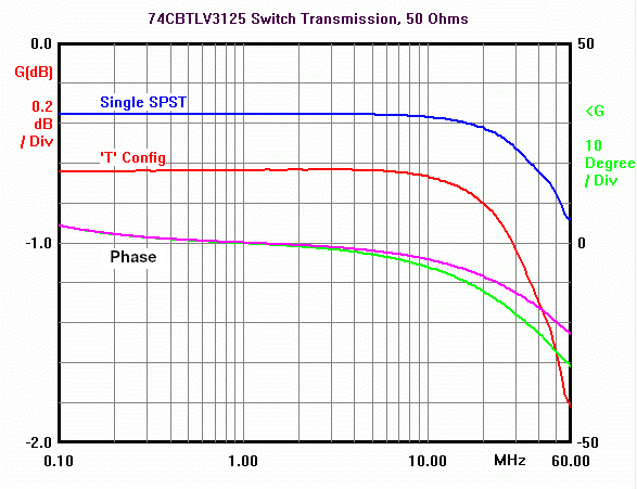
Reflection measurements showed about 1.2 VSWR up through 30 MHz. At 50 MHz, the VSWR was up to 1.4 for the single SPST and 1.7 for the "T" configuration.
Intermodulation was measured with a pair of Fluke 6060 signal generators, a Janel PD7904 Isolated power combiner and a Tek 494 spectrum analyzer. Measurements were done at both 3.8 and 14.3 MHz using a 20 kHz carrier spacing. For both frequencies, the 3rd order intercept point was about +28 dBm for the Single SPST and +25 dBm for the "T". This is high enough to allow a 2 or 3-Volt swing on transmit signals while keeping intermodulation well suppressed.
Switching speed was not measured, but it is fast and this is reflected in this series of switches being used in the various Tayloe mixing circuits. The data sheet lists the switching speed in a 3.3-Volt system at 4.4 ns maximum.
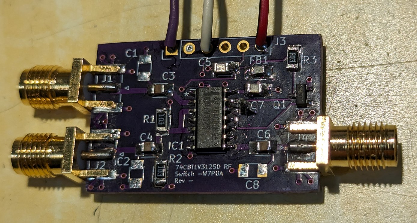
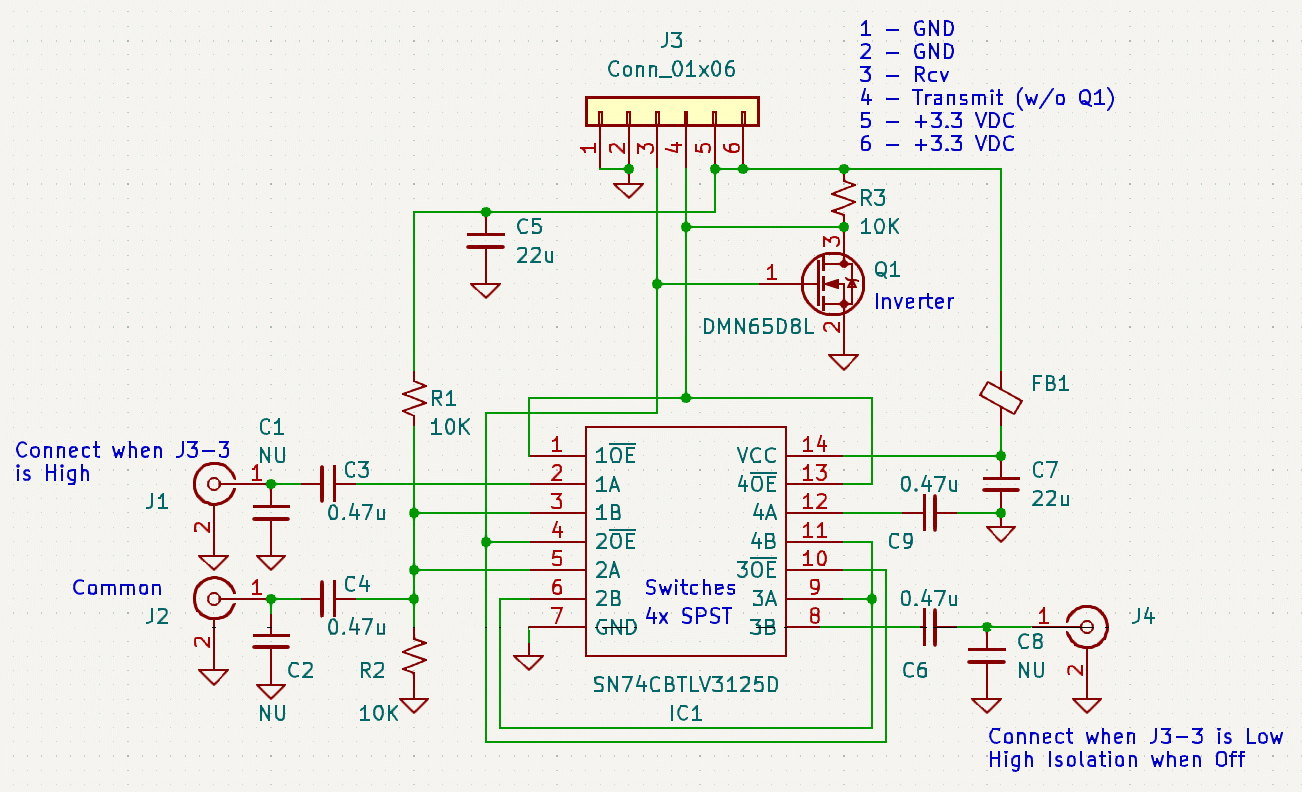
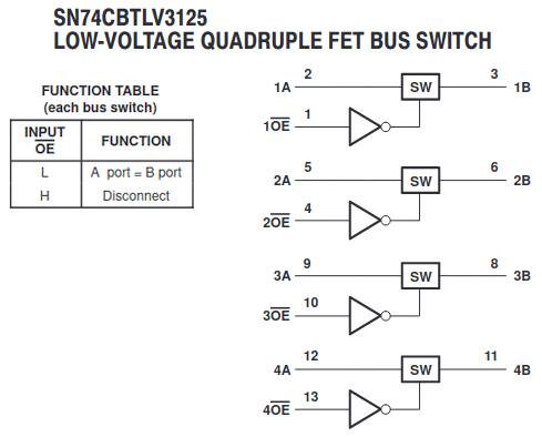
This note relates to experiments done with the 74CBTLV3125 part that has four independent SPST analog switches. There are two more parts that use the same switch element but are controlled differently. The 74CBTLV3253 has 2P4T logic that is well suited to the Tayloe mixer. The 74CBTLV3257 is 4P2T and would serve well in transmit/receive applications.
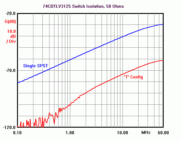
Conclusion - A pair of single SPST switches, using half of the 74CBTLV3125 provides adequate isolation (over 30 dB)) for many HF switching needs. This arrangement might handle a 2 signals for transmitting where each has a peak-to-peak maximum of 1-Volt. This is about 4 dBm for each of the two, or 7 dBm for the complete 2-Volt peak-to-peak signal. A side note is that if an extra SPST switch is not being used, it can be wired to replace the switching transistor, Q1.
Issued 22 November 2023 - All Copyright © Robert Larkin 2023