There are many simple carrier PC Boards around for the various "gain block" amplifiers such as the MSA/MRA series and the MiniCircuit ERA series. Usually, the approach is a combination of simplicity and broadband operation to make the amplifier as versatile as practical. This time, we take a different approach and include a 3-element high-pass filter (HPF) on the input and output. This has two advantages. First, it allows rejection of lower frequency signals. When received on an antenna, these can be very strong and producers of IM and harmonic interference. One example of signals to be rejected are those of the FM broadcast band at 88 to 108 MHz. The second use of the high-pass network is to improve the impedance match at specific frequencies. By starting with a standard HPF and then altering the three component values, the match can be made very good at specific frequencies. The gain-block amplifiers usually provide a reasonable VSWR of 2.0 or better, but this still can be improved considerably if multi-octave matching is not needed. Methods to achieve this are covered below.
The Circuit and Board - The circuit diagram shows the basic components.
The ERA-2 and the L and C values depend on the device and frequencies being used. This is discussed below.
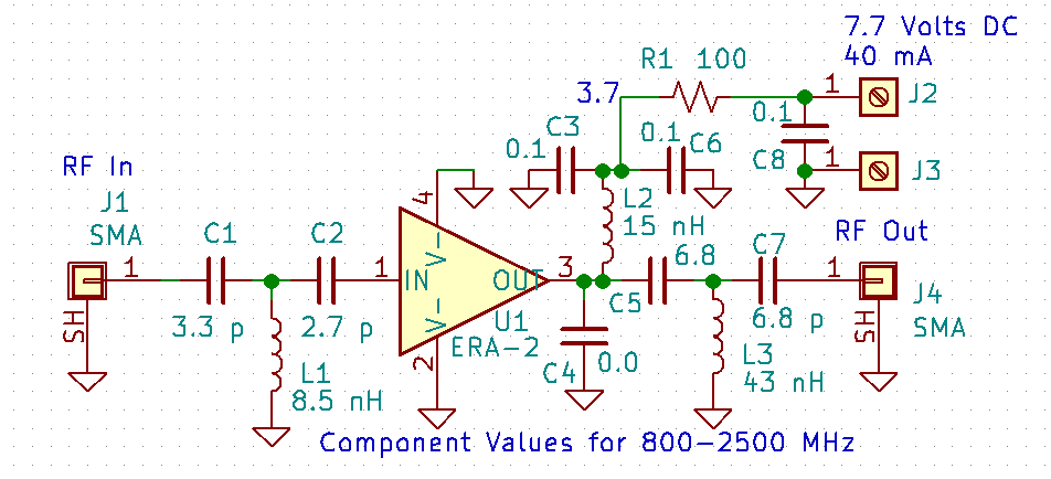
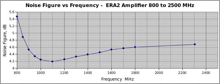
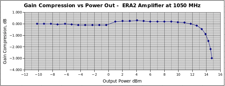
Example using ERA-2 -This design impedance matches the amplifier over an 800 to 2500 MHz frequency range covering ham bands at 903, 1296 and 2304 MHz. Performance varies with frequency with a noise figure in the 4 to 5 dB range, an an output power of around +12 dBm (15 mW) and a gain of about 16 dB. DC power is 7 VDC (or adaptable for higher) at 40 mA. The schematic shown above has the part values to support this frequency range.
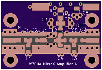
Construction consists of mounting the surface mount components, making the three coils,
and adding the SMA side mount connectors if desired or just mounting the amplifier to a metal plate if
it is a component of a larger project. The pads on the board will fit 0805 or 1206 size components.
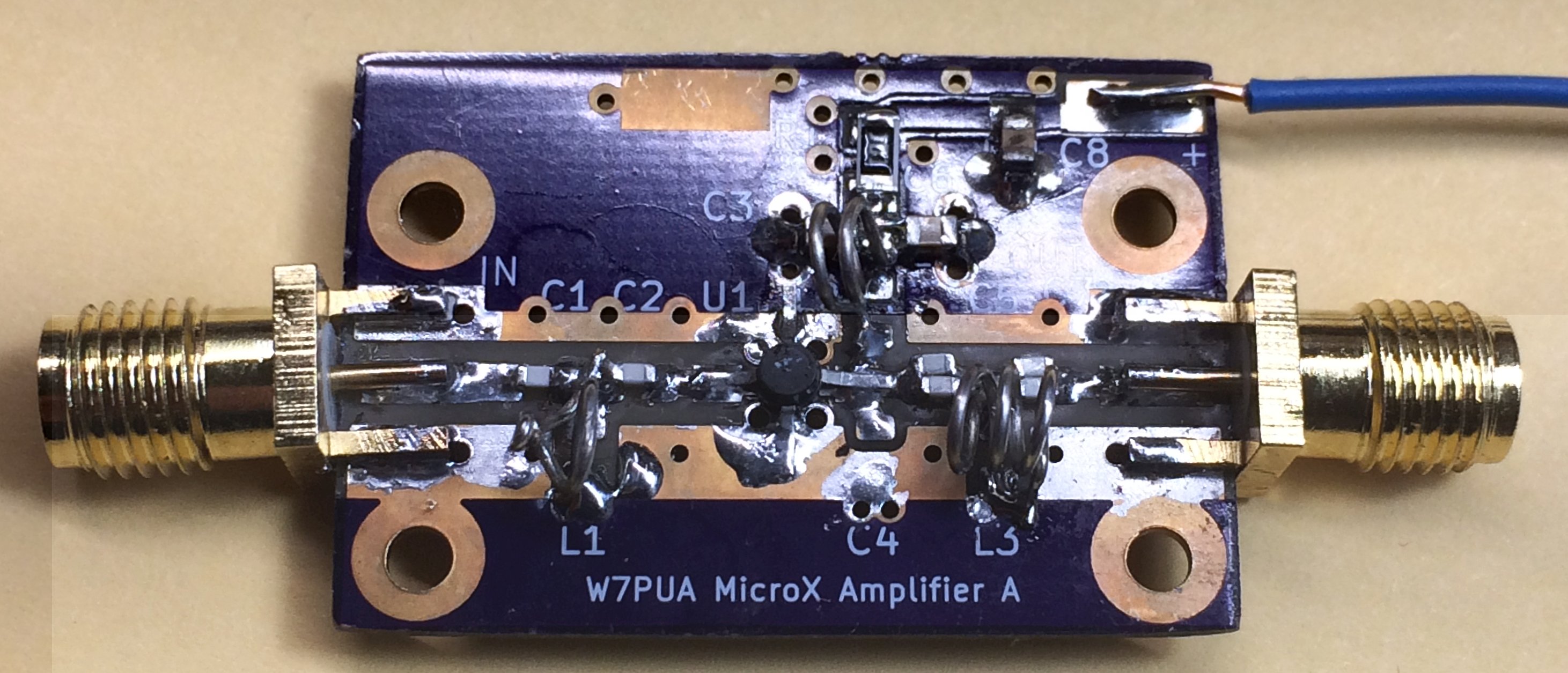
They really do not fit, but with some care, 0604 parts can be used. In the board in the picture,
a pair of 3.3 pF 0604 capacitors placed in parallel were used as substitutes for a single 6.8 pF.
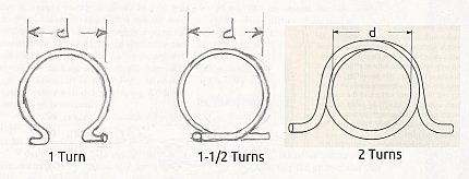
Chip inductors can be used for L1, L2 and L3. The values for this design are all low value
and I prefer to wind my own because all known values are immediately available! Additionally,
it is possible to change the value of the inductor by squeezing the turns of a home-made one.
With this amplifier the tuning of L1 is very useful.
The following illustrate the home-made inductors.
The boards from OSH Park come with a gold alloy plating. It is helpful to pre-tin the pads while being careful to not leave much solder behind. I use liquid flux, Kester 186 from a pen to make this easy. Most SMA edge connectors are for boards 1/16-inch (1.6 mm) thick. For these, they can be soldered to the thinner board on the top only, or the leads from a 1/4-Watt resistor can be used as spacers to solder the back ground-plane side.
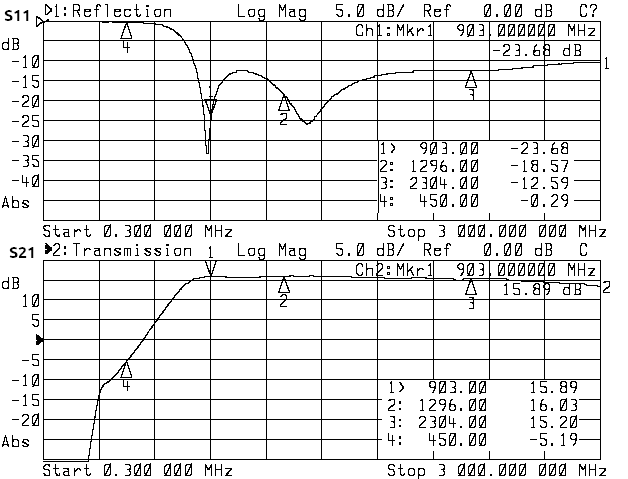
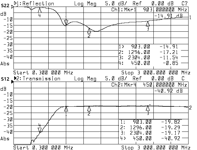
Measured Performance - The gain is quite flat across the 903 to 2304 MHz frequency range:
  903 MHz  G = 15.9 dB
  1296 MHz G = 16.0 dB
  2304 MHz G = 15.2 dB
The following graphs show the measured performance for frequencies up to 3 GHz. The terminology and order, top-to-bottom is
 S11 is the negative of the input return loss in dB
 S21 is the forward gain in dB
 S22 is the negative of the output return loss in dB
 S12 is the reverse gain in dB
The markers are 1-903MHz, 2-1296MHz, 3-2304MHz and 4-432MHz. Marker data can be read from the graphs.
Component design of the High-Pass filters - C1, L1 and C2 form one HPF for the input. C5, L3 and C7 form the HPF for the output. These can be optimized for matching, or they can be simple 50-Ohm maximally-flat filters with the cutoff frequency set lower than the operating frequency. A simple rule that keeps the added VSWR of the filter less than about 1.3 is to pick f3 = 0.5 * fop where f3 is the 3 dB point of the HPF and fop is the lowest operating frequency being used. Next the component values can be found from the following equations
 C = 3.183  / f3  pF
 L = 3.979  / f3  nH
where f3 is in GHz, L is L1 or L3 and C is C1, C2, C5 or C7. The impedance is 50 Ohms. For instance, if the lowest frequency of operation was 432 MHz, we might choose f3 = 200 MHz or 0.2 GHz. Then
  C=3.183 / 0.2 = 15.9 pF
  L = 3.979 / 02. =  19.9 nH
This is by no means the end of design possibilities. Various combinations of filter response and cut-off frequency are available. More importantly, the L and C values can be altered to improve the impedance match. The process can be done using an optimizer along with a linear circuit analysis program. That was done for the 800-2500 MHz amplifier with good results. The details of that will be saved for a later time, but what makes sense as an alternative is experimental altering of the values with measurement of gain or VSWR or noise figure. This task is simplified by working on the input network of C1, L1 and C2 and leaving the output network as the HPF just described.
Issued 4 Feb 2019 - All Copyright © Robert Larkin 2019